How to build computer chips only 3 atoms thick
Scientists describe a new recipe for making ultrathin chips that could drive see-through devices
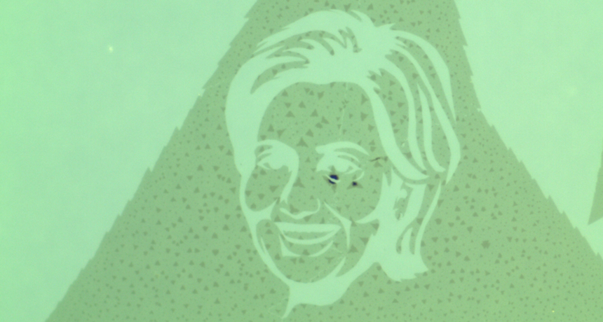
This portrait of 2016 presidential candidate Hillary Clinton is made from an ultrathin material only three atoms deep.
Stanford University
During the presidential election of 2008, clever engineers at the University of Michigan created portraits of then-candidate Barack Obama. These “nanobamas” were no ordinary pictures. They were too small to be seen with the human eye. The researchers fashioned them from rolled-up sheets of carbon atoms called nanotubes. Such nanotubes have served as building blocks for some new types of electronics.
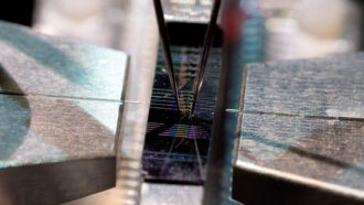
Fast forward to the 2016 presidential election. Engineers at Stanford University, in California, took a design cue from those nanobamas. For fun, they created ultra-tiny portraits of Hillary Clinton and Donald Trump. (The team also created a tiny version of the Stanford University logo.) But these engineers didn’t use nanotubes. Instead, they etched these portraits in a material called molybdenum (Mo-LIB-deh-num) disulfide, or MoS2. It’s only three atoms thick.
This is one of many super-thin materials that scientists are studying for use in future electronic devices. As devices get smaller, the computer chips that run them must shrink too. These chips process and store information. The chips in our cell phones and computers are made from a material called silicon. This element occurs naturally, which means it is found on Earth (such as in sand). Silicon also works as a semiconductor. That means it can either let electricity flow through it or block the current. Silicon computer chips have channels, or circuits etched into them to let electricity flow. That design lets these chip process and store data.
But Silicon has its drawbacks. It is a solid, notes Debdeep Jena. He studies semiconductors at Cornell University in Ithaca, N.Y. In relatively big chunks, silicon conducts electricity well. But in tiny pieces, it doesn’t. “At smaller than 50 or 60 atoms across, silicon loses the intrinsic properties that make it useful,” Jena notes. Those properties include its ability to conduct electricity.
To keep the current flowing in smaller devices, scientists must look beyond silicon. They want to find materials that work when they are only a few atoms thick. The most famous of these materials is graphene — a sheet of carbon just one atom thick. Another is MoS2. It is used as a lubricant. That means it reduces friction when two surfaces rub against each other. MoS2 occurs in nature, usually as a soft black powder. It’s also been found in narrow veins of quartz that run through granite, a type of rock. But to use MoS2 to make computer chips, scientists must make this material in a lab.
MoS2 is “an excellent semiconductor,” says electrical engineer Eric Pop. He led the Stanford team who recently described its recipe for the tiny portraits of the U.S. presidential candidates. “In some respects,” he argues, “it’s a better semiconductor than silicon.”
Why? Chips made from the super-thin MoS2 could be made much smaller than those using silicon. That means a larger number of smaller chips could be squeezed into a single device. In addition, because it is so thin, three-atom-thick chips of MoS2 would be transparent and flexible. That might make them useful for graphic displays that appear on a windshield. Or, it could turn a window into a television.
The material is not yet ready for prime time
Pop’s group has been refining its recipe on how to make MoS2 in the lab for years. It’s like cooking, he explains. “It’s a little bit of intuition and a lot of practice.” By that he means: “We play with ingredients, change the temperature a little bit.” In the end, he says, “There’s a lot of trial and error.”
Right now, it’s not easy for scientists to make useful MoS2 sheets that are so thin. Pop’s group isn’t even the first team to make this material. It is like a very small sandwich. Atoms of molybdenum, a metal, must be made to sit between atoms of sulfur.
But the group’s new recipe does point to a way to make enough thin MoS2 to build computer chips.
Atoms of sulfur must combine with the atoms of molybdenum. To make that happen, Pop and his team heat the raw materials in a furnace until they vaporize, or turn into a gas. That happens at 850° Celsius (1,562° Fahrenheit). Then, by adjusting the temperature and pressure in the furnace, the scientists can coax atoms in the gas to settle on top of a different material, called a substrate. That step is called deposition.
The key to a clean deposition is to get the atoms to line up in a way that makes sheets. This is tricky, however. MoS2 naturally forms into tiny triangles. It’s difficult to grow big triangles, and it’s difficult to stitch the small ones together.
Pop’s team created sheets of MoS2 that were about the size of a thumbnail. That may not seem large, but it demonstrates that the team’s new method works. It also makes sheets big enough to etch circuits, or channels, for an electric current to pass through. The Clinton and Trump portraits were etched outlines of circuits. The researchers reported that their test circuits set a new record for current density in MoS2 chips. (Current density is a measure of how much electricity flows through a section of the material.)
Jena says the new experiments show that MoS2 sheets can be made super-small and function as well as silicon. He adds that “Pop’s group has shown how the performance of synthetic materials is approaching that of silicon, which is very nice and encouraging.” Jena has worked with Pop in the past, although not on this project.
People likely will not see MoS2 chips in their devices for years, if not decades, Jena suspects. “We’re at a very early stage of research in this area.”
Pop’s group plans to continue to refine its recipe for making larger sheets of MoS2. Those larger sheets would enable scientists to make more chips. “The growth is limited only by the size of our furnace,” Pop says. A larger furnace would enable the scientists to make sheets bigger than the size of a fingernail. Making large sheets, which can be turned into circuits, would allow for the mass production of the material. He likens the process to baking a pizza. “How big of a pizza can you make? The biggest I can make is the size of my oven at home.”